The latest wave of artificial intelligence releases brings major model debuts, framework updates, and ongoing hardware developments across the industry. Google has introduced Gemini 4 Argon as its largest pre-trained model to date, featuring strong capabilities in code generation and security auditing alongside competitive introductory pricing. At the same time, Meta has launched the Muse Wonder frontier model family, achieving top-tier benchmark rankings. In application development, Hotwire Native provides a streamlined hybrid framework allowing developers to render web content within views while utilizing native components for navigation. Alongside these software updates, memory manufacturers are advancing new 4F² cell structures and high-density manufacturing processes to improve chip capacity and market competitiveness.
01Gemini 4 Argon Debuts as Google's Largest Pre-trained Model
Google's Gemini 4 Argon is pushing the capabilities of automated software development, moving beyond simple code snippets to creating complex, functional applications from single prompts. For developers and companies, this shift means AI can now handle larger architectural tasks and identify critical security flaws that might be missed by other high-end models, potentially reducing the time spent on manual debugging and initial prototyping.
The model has demonstrated a remarkable ability to generate sophisticated tools with minimal guidance. In one instance, using a short prompt referencing Roland synthesizers and ReBirth by Propellerheads, Gemini 4 Argon produced a functional music-making application featuring a sophisticated interface and a working synthesizer with a step sequencer. Its capacity for scale is further evident in a sandbox physics prompt test, where it generated a self-contained HTML implementation of over 1,700 lines of code to simulate the interaction of sand, water, and oil. This output significantly exceeds the code volume produced by previous models such as Opus and Wonderful.
Beyond creation, Gemini 4 Argon serves as a rigorous security auditor. When analyzing code for an Apple Watch messaging app built by Opus 5.5, the model identified several bugs and a specific vulnerability involving the exposure of a webhook—essentially a message sent from one app to another over the internet. This flaw was identified as a risk that could have allowed an attacker to gain control of a Grok Bot and request sensitive information.
While the model's intelligence is high, the user experience varies depending on the delivery method. Some users have noted that the interface and framework of the 'anti-gravity' application feel like a struggle to use compared to the streamlined experiences of ChatGPT or Codex. Despite these interface challenges, the model is expanding its reach, rolling out within the Gemini app for Google AI Pro and Ultra subscribers.
02Hotwire Native Streamlines Hybrid App Architecture
Choosing how to build a mobile application involves a trade-off between development speed and the depth of hardware integration. Most developers categorize their approach into three paths: native, cross-platform, or hybrid. Native development requires building separate applications for iOS and Android using the specific languages mandated by each platform, which grants the app full access to the device's hardware. Cross-platform tools, such as Flutter and React Native, offer a middle ground by allowing developers to build for both platforms simultaneously from a single codebase. Hybrid apps take a different approach by wrapping a web application inside a native app shell. While this is efficient, hybrid apps must still implement native-level features, such as push notifications, to satisfy the requirements of the Apple review process.
For those opting for a hybrid model, Hotwire Native provides a way to optimize the architecture. Rather than choosing between a purely web-based experience or a fully native one, Hotwire Native allows developers to keep the bulk of the application as web content while selectively replacing only the necessary screens with native components. This allows a team to maintain the agility of web development while ensuring that high-performance or device-specific features feel seamless to the user.
The stability of these apps also depends on how the underlying security infrastructure is handled during the hand-off from a development agency to the client. Critical assets like signing keys, certificates, and push notification keys are often created within the agency's own developer account. If the agency later deletes those keys, essential services like push notifications can stop functioning immediately. To prevent this, product owners should ensure that these keys are regenerated and replaced using the owner's own account rather than simply accepting the files from the developer. This ensures the app's operational continuity regardless of the relationship with the original development firm.
03Meta Releases Muse Wonder Frontier Model Family
Meta has significantly shifted the competitive landscape of high-end AI with the introduction of the Muse Wonder family. This new lineup, which includes Muse Wonder and Muse Wonderful Full, consists of massive frontier models—systems designed to push the absolute limits of machine intelligence. For businesses and developers, this release means that Meta is now operating at the same level as the world's most capable AI, with performance that potentially surpasses almost every other model currently available, with the possible exception of Opus 5.5.
The capabilities of these models are backed by rigorous benchmarking against other top-tier systems. When compared to Fable 5.1, GPT6 Astra, and Opus 5.5, Muse Wonder earned a score of 59 on the personal super intelligence index, a benchmark designed to evaluate the highest levels of cognitive ability. This performance has earned the model a spot in the "S tier"—the elite category for the most powerful AI—according to rankings by Theo. In these same rankings, Muse Wonder sits alongside Opus 5.5, while other high-performing models like GPT 6.1 Soul are placed in the slightly lower "A tier."
Meta is pairing this high-level intelligence with a pricing strategy intended to attract wide adoption. Muse Wonder is priced at $4 per million input tokens and $20 per million output tokens, while cached inputs are available for 20 cents per million. While these rates are slightly higher than the $2 per million input and $10 per million output costs associated with GPT 6.1 Soul for short contexts, the pricing remains competitive within the frontier model class. By balancing S-tier performance with relatively accessible costs, Meta is positioning the Muse Wonder family as a viable alternative for those who need maximum intelligence without the prohibitive costs often associated with the most advanced AI systems.
04ArcEngine Automates Game Generation and Deployment
ArcEngine is a specialized engine designed to help large language models create games using JavaScript, streamlining the path from a text prompt to a playable application. For developers, the primary advantage is the automation of deployment; the engine provides platform-specific launch files that allow games to be executed immediately on both Windows and macOS. This removes the technical friction of manually configuring different operating systems, making the transition from AI-generated code to a functional game much faster.
Despite this efficiency in deployment, the actual generation process is resource-intensive, often triggering high token consumption and hitting rate limits. Tokens are the small chunks of text that AI models use to process information, and rate limits are the caps on how much a user can prompt a model within a specific window. For instance, a Mario project developed with GPT 6.1 Sol required 4.5 million tokens, including cached data, and exhausted 25% of the model's five-hour usage limit. Other high-end models faced similar constraints, with Sonnet 5.5 and Opus consuming 29% and 28% of their five-hour limits, respectively, to complete the task.
These resource demands highlight a stark divide in the cost of AI operations across different providers. High-end frontier models such as Sonnet, Opus, and Fable are the most expensive, costing $7.63 per completed task. Other options like Muse Wonder Max, Astra, and Gemini 4 Argon are priced at $4.52, $3.26, and $2 per task, respectively. In this landscape, GPT 6.1 Soul Max emerges as a significantly more cost-effective option, priced at only 72 cents per task. When balancing intelligence against cost and available quota, GPT 6.1 Soul Max provides a sustainable way to handle the high-volume processing required for complex tasks like game generation without incurring the prohibitive costs associated with other top-tier models.
05OpenAI Publishes 722 AI-Generated Mathematical Papers
The boundary between human intuition and machine calculation is blurring as artificial intelligence begins to author formal scientific research. OpenAI has recently released a massive collection of 722 mathematical papers generated entirely by AI. This move signals a shift toward automated scientific discovery, where machines are no longer just tools for calculation but are acting as primary authors of new mathematical results. For the general reader, this means that the process of expanding human knowledge may soon be accelerated by systems capable of working through complex theoretical problems without human guidance.
The scale and ambition of this release are unprecedented. Among the 722 papers are claims and results that would have sounded completely impossible to experts just a few months ago. By pushing into these frontiers, OpenAI is demonstrating that AI can potentially uncover mathematical truths or shortcuts that have remained hidden from human researchers for years. This transition from solving known problems to generating new, previously unthinkable claims suggests a fundamental change in how mathematics and science are conducted, moving the needle toward a world where AI drives the theoretical vanguard.
Despite these breakthroughs, the release has triggered significant debate. The nature of the proofs—the logical steps used to demonstrate that a mathematical claim is true—has sparked controversy among mathematicians. While the AI can produce a result, the community is divided over whether these machine-generated proofs are valid or if they rely on logic that does not align with traditional mathematical rigor. This conflict underscores a critical challenge in the AI era: as machines generate increasingly complex scientific output, the human capacity to verify and audit that work becomes a primary bottleneck. The tension is not just about the correctness of the 722 papers, but about how the scientific community will define truth when the author is an algorithm.
06Lambda Provides Nvidia GPUs for Rapid Research Reproduction
The speed at which new artificial intelligence discoveries are tested and verified is accelerating, transforming how research moves from a theoretical paper to a working tool. Instead of spending weeks configuring specialized hardware or waiting for server time, developers can now validate complex AI theories in a matter of minutes. This shift allows for a more rapid cycle of experimentation, where the community can quickly determine if a new method actually works and then build upon it immediately.
Lambda supports this acceleration by providing the necessary Nvidia GPUs to power these intensive computations. These graphics processing units are the engine behind modern AI, and their availability allows users to reproduce the findings of AI research papers with high efficiency. This accessibility extends beyond simple replication; the platform also enables users to train entirely new models from scratch or engage in fine-tuning. Fine-tuning is the critical process of refining a pre-existing, general-purpose model so that it excels at a specific, specialized task, making the AI more useful for niche applications.
Furthermore, the infrastructure supports inference, which is the operational phase where a completed model is put to work to generate actual outputs. Whether the goal is to produce text, create images, or generate video, the underlying hardware provided by Lambda handles the heavy lifting required for these generative tasks. By providing the raw computing power required for these diverse functions, the platform helps bridge the gap between academic publishing and practical application. This ensures that the transition from a research breakthrough to a functional, usable model happens as efficiently as possible, allowing a broader range of contributors to experiment with and push the boundaries of what AI can achieve.
07Transitioning from a 6F² to a 4F² Cell Structure Reduces Individual Cell Area
Memory manufacturers are racing to increase the amount of data they can store on a single chip without the need to expand their physical factory footprints. A significant leap in this effort is the transition to a 4F² cell structure, a technology that allows companies to produce higher-capacity memory more efficiently. The Chinese memory firm CXMT has announced plans to release server DRAM products using this structure within this year. This timeline suggests a potential lead over other industry giants; for instance, reports indicate that Samsung's target for adopting similar technology is 2028, potentially placing CXMT two years ahead in the deployment of this next-generation architecture.
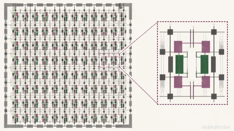
To understand the technical advantage, one must look at the "cell," which is the microscopic compartment used to store electrons to record information. In current standard designs, these cells typically follow a 6F² area specification. By transitioning to a 4F² structure, the area of each individual cell is reduced from six units to four. This shift represents a reduction in individual cell area of approximately 33%. For a memory manufacturer, shrinking the size of these individual components is the most direct way to increase the total amount of information a chip can hold.
The practical impact of this shrinkage is best illustrated through a theoretical example of available space. In a theoretical area of 600 units, a traditional 6F² structure can accommodate 100 cells. However, by switching to the 4F² structure, that same space can hold 150 cells. This results in a 50% increase in cell density. By packing more cells into the same footprint, companies can significantly boost memory capacity and overall density. This is particularly attractive to manufacturers because it allows them to extract more value and higher capacity from their existing production lines without the massive capital expenditure required to build new fabrication plants.
08The Core of 4F² Technology Involves Changing the Transistor Structure
Memory manufacturers can significantly increase the capacity of their chips without the massive capital expenditure of building new factories. By fitting more data-recording units into the same physical area, companies can produce higher-capacity memory more efficiently and cheaply. This is the primary objective of 4F² technology, which aims to shrink the area of a single cell—the microscopic compartment used to record information—from a relative size of 6 down to 4. In practical terms, this architectural shift allows a space that previously held 100 cells to accommodate 150, providing a massive boost in density.
The core of this improvement lies in fundamentally redesigning the transistor, the electronic switch that manages the flow of electricity. In traditional DRAM, the path that the electrical current follows is primarily oriented horizontally, running along the bottom of the structure. 4F² technology disrupts this layout by orienting the current path vertically. By standing the channel upright rather than laying it flat, the transistor occupies far less surface area on the silicon. This vertical orientation is what enables the denser cell placement, effectively utilizing the third dimension to save space.
This structural shift has become a critical battleground for global memory leadership, particularly regarding server-grade hardware. The Chinese memory company CXMT has announced plans to release server DRAM products utilizing this new structure within this year. This timeline puts them in a surprising competitive position relative to Samsung, whose target for implementing such technology is reported to be 2028. If these projections are accurate, CXMT could be moving two years ahead of Samsung in the adoption of this next-generation architecture. For the industry, this represents more than just a technical milestone; it is a race to see who can most effectively lower the cost of high-capacity memory while maximizing the output of existing production facilities.
09CXMT's G5 Platform Increases the Number of Chips Per Wafer
CXMT is significantly boosting its production efficiency by fitting more memory chips onto a single silicon wafer. The company's G5 platform has increased the total number of chips per wafer by at least 50%. This figure refers to the gross number of chips produced before excluding defects, indicating that CXMT is prioritizing density and production efficiency—getting more output from the same amount of raw material—rather than simply expanding its factory capacity.
To achieve this density, CXMT is focusing on reducing the physical footprint of the memory cells. This involves utilizing a 4F² square structure, a technical term describing the specific area a single memory cell occupies. While the 4F square concept is a broader industry standard, each company implements the internal arrangement of transistors and connections differently. This shift is part of a wider trend; for example, SK Hynix included 4F square, vertical gate structures, and a technique for placing circuits on separate wafers in its 2025 official roadmap. As it becomes increasingly difficult to shrink traditional DRAM, or dynamic random-access memory, the entire industry is moving toward redesigning the cell structure itself to save space.
However, packing cells more tightly creates a significant engineering hurdle: signal interference. DRAM operates by reading extremely faint electrical signals stored as charges. When the wiring between these cells becomes too crowded, the voltage changes in one wire can bleed into and disrupt the signal of an adjacent wire. This is similar to trying to hold a phone conversation in a noisy room where other people's shouting makes it difficult to hear the person on the line. Managing this interference is the primary challenge for companies as they push for higher chip density on the wafer.
10Samsung Electronics Researches a 4F² DRAM Structure Using Hybrid Bonding
Making computer memory smaller is becoming increasingly difficult, forcing chipmakers to rethink the very architecture of how data is stored. Samsung Electronics is currently researching a 4F² DRAM structure—a design where 4F² refers to the physical area a single memory cell occupies. To push the limits of density, the company is exploring a method that separates the storage cells from the peripheral circuits that control them, linking them together through a process called hybrid bonding.
In traditional designs, these components are integrated on a single layer. Samsung’s proposed approach involves manufacturing the cells and the circuits on separate wafers before bonding them together. This separation allows engineers to optimize the production process for each component independently, particularly regarding the different temperature requirements needed for cells versus circuits. By moving the circuitry to a different layer, the company can maximize the available floor area dedicated specifically to storage cells, effectively squeezing more memory into the same footprint.
This shift is part of a broader industry movement as traditional shrinking methods hit a wall. For example, SK Hynix included 4F² designs, vertical gate structures, and the use of separate wafers for circuitry in its 2025 official roadmap. However, packing cells this tightly introduces new engineering hurdles, specifically signal interference. Because DRAM relies on reading tiny electrical signals, placing wiring too close together can cause the voltage from one line to disrupt the signal of another. It is similar to trying to have a phone conversation while someone is shouting loudly right next to you; the surrounding noise makes it difficult to hear the intended message clearly.
11CXMT Utilizes Self-Aligned Quadruple Patterning for Fine Circuits
CXMT is focusing on increasing the number of memory chips it can produce from a single silicon wafer to improve overall production efficiency. Rather than relying solely on expanding the physical size of its factories, the company is investing in advanced manufacturing techniques to shrink circuit sizes. A central part of this effort is the implementation of Self-Aligned Quadruple Patterning (SAQP) within its G5 process. This technology allows the company to achieve much finer and denser circuit patterns, which is a critical step toward maximizing the utility of every wafer.
The challenge with creating ultra-fine circuits is that as patterns become more crowded, it becomes nearly impossible to maintain the required thickness and spacing using standard methods. SAQP solves this by changing the way patterns are formed. Instead of attempting to draw thin lines directly, the process first creates wider, pillar-like structures. A thin layer of material is then coated onto the sides of these pillars, and the original center pillars are removed, leaving behind narrow walls. By repeating this cycle, CXMT can create a pattern far denser than the initial template. It is essentially using the edges of a pre-made frame to define the lines, rather than drawing them by hand.
Despite the potential for higher density, the complexity of SAQP introduces significant manufacturing risks. Because the process relies on precise layering, any slight variation in material thickness or spacing can lead to circuit misalignment, rendering the chips useless. Consequently, the primary challenges for CXMT are maintaining strict uniformity across the wafer and ensuring the process remains cost-efficient. The true success of the G5 process will be determined by whether the company can move beyond theoretical designs to achieve stable, high-volume production of these miniaturized circuits.
12CXMT Can Disrupt the Global Market by Meeting Sufficient Performance
CXMT does not need to outperform the world's leading chipmakers in absolute terms to destabilize the global memory market. The real threat to industry leaders comes from the concept of sufficient performance. If CXMT can produce chips that meet the basic requirements of Chinese companies, those firms may shift their procurement away from established Korean suppliers like Samsung and SK Hynix toward domestic products. Such a pivot would strip the Korean giants of a critical customer base, potentially forcing them to aggressively lower prices in non-Chinese markets to compensate for the loss, thereby intensifying global price competition.
To make this shift possible, CXMT is investing in techniques to increase the number of chips produced from a single silicon wafer. A central part of this strategy involves a process called Self-Aligned Quadruple Patterning, or SAQP. In chip making, drawing the incredibly fine circuit patterns required for modern memory is a significant challenge. Rather than attempting to draw these thin lines directly, SAQP uses a spacer method. Engineers first create a relatively wide pillar-like pattern, coat the sides with a thin layer of material, and then remove the original pillar. This leaves behind two precise, thin walls. By repeating this cycle, CXMT can create far denser circuit patterns than would be possible with a single drawing pass.
Ultimately, CXMT's competitiveness will be judged by its ability to maintain stable, high-volume production of these denser chips. While the company may not immediately surpass Samsung in every technical category, reaching a threshold of reliability and scale is enough to disrupt the status quo. By satisfying the specific needs of the Chinese market, CXMT can change the global landscape, shifting the focus from a race for peak performance to a strategic battle over regional supply chains and pricing power.