Imagine an autonomous vehicle exiting a pitch-black tunnel into the blinding glare of a midday sun. In that split second, the vehicle's visual system must transition from amplifying microscopic photons to filtering out overwhelming noise without losing track of a pedestrian in the periphery. For years, the industry has attempted to solve this by stacking multiple sensors—one for visible light and another for infrared—but this approach creates a computational bottleneck. Every additional sensor adds a stream of raw data that the onboard processor must synchronize and analyze in real-time, increasing latency and power consumption at the exact moment when millisecond decisions are critical.
The Hybrid Architecture of Organic and Quantum Dots
A joint research team led by Professor Jae-won Shim from the Department of Electrical and Electronic Engineering and Professor Seung-ju Oh from the Department of Materials Science and Engineering at Korea University, alongside Dr. Min-cheol Park from the Next-Generation Semiconductor Research Institute at the Korea Advanced Institute of Science and Technology (KIST), has introduced a solution that collapses these functions into a single device. They have developed an organic/quantum dot (QD) single-type photodetector. By integrating organic semiconductors with quantum dots—nanometer-sized semiconductor crystals—the team created a hybrid structure capable of dual-spectrum detection.
The core innovation lies in the operational mechanism: the device distinguishes between visible and infrared light signals simply by switching the polarity of the applied voltage between positive (+) and negative (-). This allows a single sensor to act as a selective filter, extracting specific wavelengths without the need for external optical filters or the physical swapping of hardware. This capability is particularly vital for sectors requiring high-precision dual-spectrum imaging, such as non-invasive medical diagnostics, optical communications, and advanced robotics.
Solving the Interface Noise Problem Through Phase Separation
The technical breakthrough that enables this sensitivity is a process called vertical and horizontal phase separation. In traditional dual-spectrum detectors, engineers typically insert a charge transport intermediate layer to manage the flow of electrons between different materials. However, these layers often introduce interface noise—electrical interference that occurs at the boundary where two different materials meet—which degrades the signal-to-noise ratio and limits the sensor's ability to detect ultra-weak light.
The Korea University and KIST team bypassed this requirement entirely. By controlling the phase separation, they forced the organic materials and quantum dots to self-align in specific vertical and horizontal orientations. This architecture allows the active layer—the part of the sensor that absorbs light and converts it into electricity—to perform its own self-filtering. By removing the intermediate layer, the team suppressed interface noise and simplified the device structure, turning the material's own physical arrangement into a functional filter.
The performance metrics validate this structural shift. The photodetector reduced light interference to approximately -80 dB in the visible light spectrum and -60 dB in the short-wave infrared (SWIR) spectrum. In terms of specific detectivity, a standard measure of a sensor's sensitivity to weak light, the device recorded 4.3 × 10^12 Jones in the 710 nm visible light region and 6.4 × 10^11 Jones in the SWIR region. Furthermore, the linear dynamic range—the span of light intensity the sensor can accurately perceive—was expanded to cover areas 100 times darker than those detectable by conventional sensors. Notably, the team maintained this high sensitivity even while increasing the active layer thickness beyond the industry-standard 200nm, challenging the long-held design belief that increased thickness inevitably leads to performance degradation.
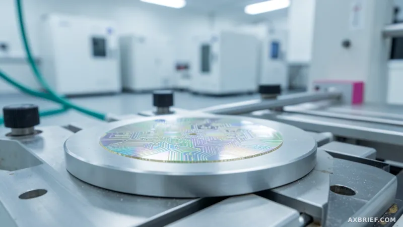
To demonstrate the practical utility of this technology, the researchers applied the sensor to a silicon wafer alignment process. Silicon wafers reflect visible light on the front side but allow infrared light to pass through the back. By simply switching the voltage, the team was able to identify both the front and back patterns of the wafer, achieving physical alignment within an extremely fine margin of error. This proves that high-precision alignment in 3D semiconductor stacking and packaging can be achieved through electrical control rather than expensive, bulky optical equipment.
This research, published on June 12 in Nature Communications (IF=15.8), provides a scalable foundation for the next generation of vision systems that must operate seamlessly across the electromagnetic spectrum.