Every time you query a search engine, trigger a translation, or prompt a generative AI model, you are initiating a massive, invisible sequence of matrix multiplications occurring deep within a data center. While the user experience lasts only a few seconds, the physical infrastructure beneath it is performing trillions of calculations. At the center of this computational storm is Google’s Tensor Processing Unit (TPU), a specialized hardware architecture designed specifically to accelerate the mathematical heavy lifting that powers modern artificial intelligence.
The 121 Exaflops Benchmark
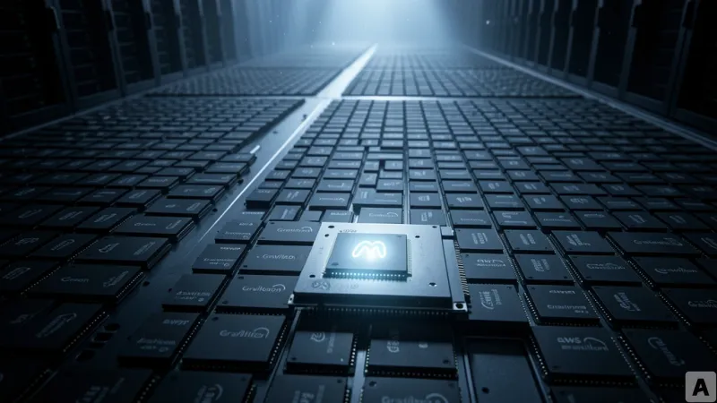
Google has officially disclosed the performance metrics for the latest generation of its TPU infrastructure, setting a new bar for AI-specific compute. The latest iteration delivers 121 exaflops—a staggering capacity of 100 quintillion operations per second. This performance leap is supported by a doubling of memory bandwidth compared to previous generations, a critical requirement for feeding data to increasingly large model parameters. These specifications, detailed in the TPU official technical documentation, represent the new baseline for enterprises attempting to train and deploy frontier-level models without hitting the physical bottlenecks of traditional hardware. By optimizing the hardware design specifically for the iterative nature of neural network training and inference, Google has effectively increased the compute density available to its internal and cloud-based workloads.
Why Custom Silicon Outperforms General-Purpose GPUs
For years, the industry relied on general-purpose graphics processing units (GPUs) to handle the surge in AI demand. However, the market has shifted toward domain-specific architectures as the standard for high-performance AI. While a general-purpose chip must balance a wide array of tasks—from rendering graphics to general floating-point math—the TPU is architected exclusively for the matrix operations that define deep learning. This structural focus allows for significantly higher computational efficiency per watt, which translates directly into lower operational costs for large-scale model deployment. As outlined on the Google Cloud TPU introduction page, Google has spent over a decade refining this hardware from the ground up, moving away from the constraints of general-purpose silicon to create a vertically integrated stack that prioritizes AI throughput above all else.
The Business Impact of Data Center Efficiency
For developers and enterprise architects, this shift in hardware capability manifests as a dramatic increase in inference speed and deployment flexibility. When an organization can run larger, more complex models with fewer physical resources, they gain a distinct strategic advantage in both latency and cost-per-token. This hardware-level optimization enables real-time, complex reasoning capabilities that were previously too expensive or slow to implement in production environments. By maintaining its own proprietary chip ecosystem, Google has successfully reduced its reliance on third-party hardware vendors, securing total control over its computational destiny and the scalability of its AI services.
Computational efficiency at the hardware level has become the primary determinant of software intelligence.