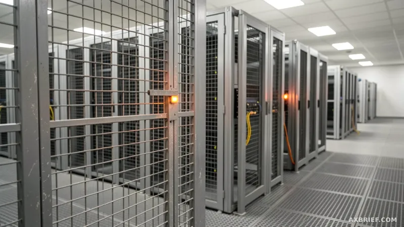
Modern data centers are currently locked in a brutal war of attrition, fighting a battle against the laws of physics. Every time a Large Language Model generates a single token, a massive amount of data must travel a circuitous route from memory to the CPU and then to the GPU, only to return again. This constant movement, often described as a data relay race, creates a catastrophic bottleneck where the fastest chips in the world spend a significant portion of their time simply waiting for data to arrive. The result is a staggering waste of electricity and a physical footprint that requires thousands of server racks to maintain performance.
The Financial and Technical Blueprint of MX1
This inefficiency has created a massive opening for XCENA, a company that recently secured 135 million dollars in a Series B funding round. The investment, which brings the company's total funding to 185 million dollars and its valuation to 570 million dollars, was led by Altnum and IMM Investment, with participation from Costone Asia, SBI Investment, and Mirae Asset Capital. The capital is backing a leadership team with deep roots in the semiconductor industry, including CEO Jin Kim, CTO Do-hoon Kim, and CPO Joo-hyun Kim, all of whom bring experience from Samsung Electronics and SK Hynix.
At the center of this investment is the MX1 chip, a piece of hardware designed to fundamentally alter the server rack. XCENA claims that implementing the MX1 can allow a single server to handle the workload that previously required ten. The technical mechanism driving this efficiency is Compute Express Link (CXL), a high-speed interconnect that allows the processor and memory to communicate with far less friction. By utilizing CXL, the MX1 integrates computational capabilities directly into the DRAM (Dynamic Random Access Memory), effectively moving the processing power to where the data lives rather than forcing the data to travel to the processor.
For hyperscalers who spend tens of billions of dollars annually on infrastructure, the MX1 targets the most expensive overheads: pre-processing, data caching, and the management of KV (Key-Value) caches. In traditional setups, the CPU handles these orchestration tasks, which drains resources and slows down the overall pipeline. The MX1 offloads these specific tasks to the memory module itself, ensuring that the GPU can remain focused on high-load matrix multiplications without being throttled by data delivery delays.
The RISC-V Pivot and Vertical Integration
While other industry players like Marvell and Astera Labs have pursued similar goals, XCENA has taken a radically different architectural path. Most competitors rely on a small number of powerful, general-purpose cores to manage data. XCENA has instead opted for a massive array of thousands of tiny, optimized cores based on the RISC-V open-source instruction set architecture. By utilizing thousands of small cores rather than a few large ones, the MX1 achieves a much higher density of computation per square millimeter of silicon while maintaining superior power efficiency.
This design choice is supported by a strategy of total vertical integration. While many chip designers license external Intellectual Property (IP) for their internal components, XCENA has designed its own internal memory hierarchy, interconnect buses, and DRAM controllers from the ground up. This level of control allows them to minimize transmission latency at a granular level, creating a custom-tailored path for data that general-purpose chips cannot match. The tension here is between flexibility and efficiency; by sacrificing the general-purpose nature of the cores, XCENA has maximized the throughput for the specific patterns of AI data movement.
This shift represents a move away from the traditional Von Neumann architecture, where the separation of processing and memory is the primary constraint. By treating memory as an active participant in computation rather than a passive storage bin, the MX1 transforms the memory module into a co-processor. This effectively removes the CPU from the critical path of data orchestration, solving the bottleneck not through faster speeds, but through shorter distances.
Production of the MX1 is slated to take place through Samsung Electronics' foundry lines. The company expects to complete the fabrication process by the end of 2026, with commercial availability and revenue generation beginning in 2027. The target market remains the hyperscale data center operators, for whom a marginal increase in memory efficiency translates into hundreds of millions of dollars in operational savings.
The ability to compress ten servers into one does more than just save space; it fundamentally alters the cost structure of AI services. As the industry moves toward a future of autonomous agents and real-time reasoning, the competitive edge will no longer be defined by who owns the most servers, but by who possesses the highest processing density per watt.